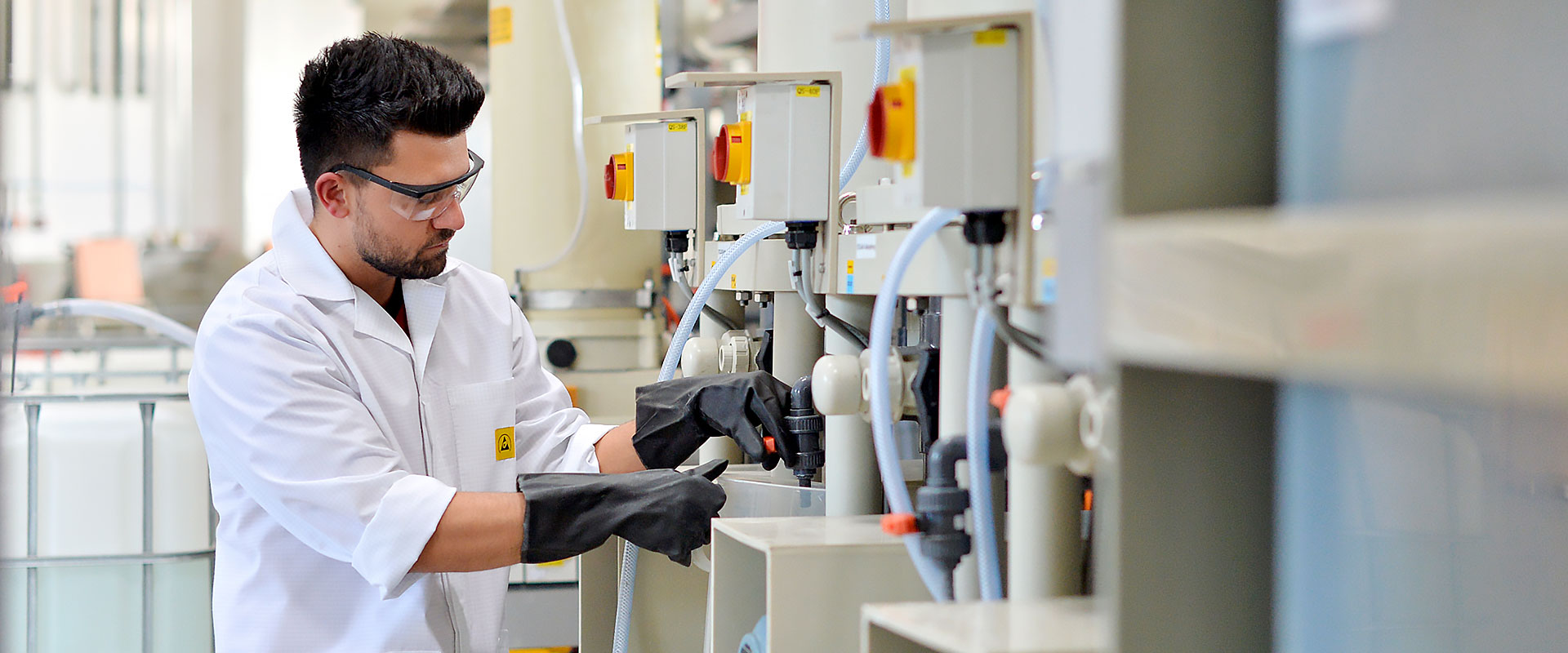
Technologies

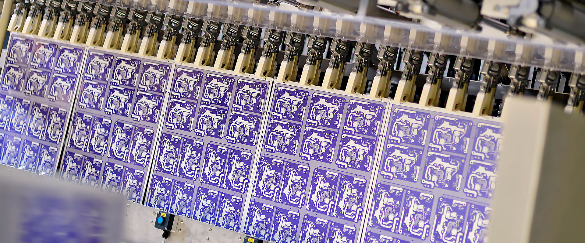
Circuit boards are the core of electronic appliances. Etched conductor paths enable electrical connection between components.

Depending on their final use, these boards can satisfy totally different requirements, which means that their execution can be completely different.

To achieve this diversity in best quality, our production process is subject to the following standards and specifications:

Basis Material

We have a permanent stock of the standard basis material FR4. Furthermore, on request we can procure further variations of FR4 material, also in different thicknesses.

We process basis material in thicknesses from 0.50mm to 3.2mm, copper end thicknesses to 135µ with comparative tracking index (CTI) values to max 600 volts and a TG value of 150 degrees Celsius.

DescriptionNEMAIPC-4101Tg C°CTE <
Tg ppm/K
CTE >
Tg ppm/K
Zersetzungs-
temperatur C°
T260 minT288 minEigenschaft
epoxy-paper-glass CEM1 10 100 - - -      
epoxy-glass FR4 21 135 70 270 310 20 3 standard
epoxy-glass FR4 24 150 70 270 310 20 3 higher Tg
epoxy-glass FR4 94 150-200 70 270 310 20 3 low halogen
epoxy-glass FR4 99 150 45 240 325 30 5 therm. Filler
epoxy-glass FR4 124 150 45 230 325 30 5 therm. Filler

Data Format

We process the following data formats:

  • Layout Data:
    standard format
    • Gerber 274x
    • Eagle
  • Further Formats:
    • Gerber
    • ODB++
  • Drill and Routing Data:
    • Excellon (standard format for all drilling data)
    • Drillfile in Sieb & Meyer Format 3000

Quality

Quality standards
Our circuit boards are constructed to meet IPC-A-600 class 2, or class 3 norms. We can also produce according to the following standards:

  • PERFAG 1
  • PERFAG 2
  • PERFAG 3
  • IPC-SM-840
  • IPC-R-700
  • IPC-A-600
  • IPC-6012
  • IPC-2221

Quality Management
MicroCirtec is DIN EN ISO 9001 and UL© certified.

Production parameters, production conditions and raw materials are evaluated and registered with calibrated measuring instruments.

Test Procedures
The quality of the circuit boards is checked continually during production in the following ways:

  • Non-destructive test

Automatic and optical tests are conducted according to IPC-A 600, class 2. If required, specific test procedures can be adapted at any time to other specifications.

  • Destructive test
    • Micro section (to assess electrolytic copper deposition and thickness of the surface protection layer.
    • Adhesion test
    • Pressure cooker test (multilayers are regularly subjected to thermal shock tests)
  • Parameter documentation
    Automatic identification and storage of the following parameters for 10 years:
    • Production parameters
    • Quality-bound results
    • Time management, including the respective worker
  • Electrical tests
    In the final eIectrical test circuit boards are checked for breaks and shorts. (>10 Ohm: break: <10 MegOhm:short)
    MicroCirtec tests with the following test:
    • Test adaptor/Parallel tester
    • Finger test/Flying probe
  •  X-Ray
    X-Ray fluorescence spectrometry to measure layer thickness and analyse materials (metals).

Design Guidelines

Our guidelines are here to ensure functionality, high quality and economic circuit board design to satisfy your and our quality demands. The most important parameters and characteristics are combined in a detailed download.

Our competent sales and distribution department is here to advise and serve you personally in the setup of your individual circuit board designs.

Please contact us!

Layout

The layout of a circuit board is crucial for the functionality of electronic circuits, and, therefore, for the final product. Our experienced sales and distribution experts and our in-house CAM department work hand in hand from the very beginning to support the implementation of your layout. MicroCirtec ensures strict adherence to your specifications. Even if our feasibility test points out potential for optimization, our specialists, after consulting you, can still manufacture your design. Our CAM department also provides advice for board setup, also regarding financial matters.

Mechanics

We bore, rout and score your circuit boards according to your data and wishes.
The mechanical processing method is dependent on your individual specifications, the order size and your data. We work with modern, fully automatic CNC drilling and routing machines.

Scoring (V-routing)
The mechanical technique with the least material wastage when processing rectangular plates or boards, and straight outer contours is the so-called curb routing or scoring.

The circuit boards are positioned above and below a respective scoring tool. CNC driven, a depth-defined groove is routed into the material leaving a fixed tab or a predetermined breaking point. The board can be separated manually or with a panel separator along this furrow immediately, or after further processing, e.g. mounting.

The advantage: no space is needed for a routing machine, therefore the circuit boards can be laid at “0-distance” so that scoring is a cost-effective alternative for large volume orders.

Contour Routing
As an alternative to scoring, MicroCirtec offers contour routing. The advantage over scoring is that outer contours can be processed in special ways, for instance, round, oval, waved, zigzag, etc. The following should be noted:

  • If PCBs are ordered as panalized by routing, a space of 2,0mm within the bare board is usually sufficient to place fixing tabs between the individual plates.
  • If the order is placed as single board, a space of min. 8,0mm between plates must be allowed in order to separate the individual circuit boards.

Mixed variations of both mechanical finishing methods are also usual. We are happy to advise you as to which method is best for you.

Prints

The classical colour of a circuit board is green. The colour is achieved by applying so-called solder resistors which we also offer in white, red, blue and black in addition to green.

Solder resistors serve initially to protect the copper structures from oxidation and from damage to the surface.

The solder-resist coating is carried out by a photo-printing process whereby a special varnish polymerised by UV-light is applied to the circuit board surface (methods used are casting or screen printing) and, finally, exposed photo technically. The non-polymerised component parts exposed remain water soluble and, even in micro-meter zones, are developed with sharply defined contours. A final thermal curing follows to achieve the required electro-physical characteristics of the varnish.

MicroCirtec uses solder resistors based exclusively on epoxy resin as this further improves creep-resistance on the surface of the circuit board.

Surfaces

We apply all types of finishing, such as:

  • Hot Air Levelling Leadfree (HAL)   
  • Chemical Nickel Gold (NiPAu or ENIG)
  • ENEPIG (Electroless Nickel Electroless Palladium Immersion Gold) 
  • Chemical Tin (Chem.Sn)
  • Chemical Silver (Chem.Ag) 
  • Hard Gold Plating and OSP (Organic Surface Protection)
  • Galvanic goldfinger plating
VerfahrenHALchem.
SN
chem.
Silber
OSPchem.
Ni/Au
Hartgold
Metall/Legierung Sn0, 7CU
Sn0, 7Cu0, 1Ni
Sn98, 2Ag0, 3Cu0, 7Ni0, 02
Zinn Silber Organic 99,9Au 99,5Au
Schichtstärke µ <10 <1 02,-0,4 0,02-0,06 0,05-0,12 Au
/4-8 Ni
0,8-5 Au
Planarität befriedigend sehr gut sehr gut sehr gut sehr gut sehr gut
Lagerfähigkeit bei
stabilen Konditionen
≤ 12 Monate < 6 Monate < 6 Monate < 6 Monate < 12 Monate < 12 Monate
Mehrfachlötbarkeit sehr gut befriedigend gut bedingt sehr gut -
reaktivierbar ja ja ja ja bedingt bedingt
Al-Draht-Bonden nein nein bedingt nein ja -
Au-Draht-Bonden nein nein nein nein nein -
Drucktasten-Kontakt nein nein nein nein ja ja
Einpresstechnik ja ja ja nein nein nein

Hot Air Levelling (HAL)

The term hot air levelling is used both for the production procedure as well as for the surface of circuit boards with 99.55% Sn (tin), 0.3% Ag (silver) and 0.15- 0.05% Ni (nickel). It protects the underlying copper drilling holes from oxidation.

The circuit boards are dipped into a hot melt (<260°C) of the above metals. The surfaces are then levelled with compressed hot air and the drilling holes blown free. The surface is very well suited for multi–soldering, and storage is possible for up to 12 months.

Radial mounting with one-sided SMD technique is both qualitatively and financially attractive using HAL. Our solder is lead-free and meets RoHS regulations.

Chemical Nickel Gold (ENIG = Electroless Nickel immersion Gold)

ENIG or chemical nickel gold is a metallic, easy to solder surface. It is deposited onto the copper layer of the soldered points at a strength of 4 – 9µ nickel and, ideally, 0.05 – 0.1µ gold which prevents oxidation of the copper. The electroless plating is deposited by means of catalytic processes, as well as the electrical potential difference (valency) of the metals utilised.

The surface is completely level, suitable for multi-soldering with SMD, Cob and HDI techniques, as well as aluminium wire bonding, and can be stored for up to 12 months.

The surface is IPC-4552 specified and meets the current RoHs and WEE requirements.

ENEPIG (Electroless nickel electroless palladium immersion gold)

The ENIG procedure adds an electroless layer of palladium (0.05 – 0.25µ thick) to the final surface between the nickel and gold processing steps.

This additional layer is not only excellent for all varieties of soldering, but is used predominantly for gold wire bonding. This method is seen as a very expensive special application.

Chemical tin

Chemical tin is a metallic, easy to solder final surface. A fine electroless layer of approx 0.7 – 1.2µ tin is deposited onto the copper soldering points where it prevents oxidation of the copper. The surface of the pad is very smooth and is therefore particularly suitable for SMD-CoB and HDI and moulding.

Storage should not exceed six months. Dampness and temperature changes during storage can impair the solderability.

Chemical Silver (chem. Ag.)

Chemical silver is a metallic, excellent for multi-soldering final surface with a layer measuring 0.2 – 0.4µ of electroless plating onto the solder points (similar to the chemical tin process). The surface is smooth and is well suited for SMD moulding.

Storage of up to six months is possible. Similarly to chemical tin, temperature changes and dampness cause surfaces to lose solderability. Surfaces should on no account have contact with sulphurous materials (e.g. certain types of packing paper).

OSP (Organic Surface Protection)

OSP is an organic solution that is selectively deposited onto solderable copper surfaces at a layer strength of 0.2 – 0.6µ by means of dipping or rinsing baths. The surface is smooth and well suited for a fine SMD mounting. Multiple solderings are not possible as the transparent layer disintegrates above 150°.

Storage is limited to 6 months maximum.

Galvanic goldfinger plating

In contrast to electroless gold (=ENIG procedure), nickel is also used as a copper diffusion barrier but the gold is deposited by anode-cathode electrolysis. Thus, significantly greater thickness layers of 1 - 4µ can be achieved as the deposition is not dependant on the different electric potential of nickel and gold. This “hard gold” is used for circuit boards with edge connectors with multiple plugs. The thicker the gold, the higher the number of mating cycles (e.g.: 0.4µ Au = 20 mating cycles, 2µ = 500 mating cycles).

subscribe to our newsletter